TECHNOLOGY DEEP DIVE
Sensors, architectures, advantages, and applications
CMOS Image Sensor (CIS)
Technology Overview
Our CMOS Image Sensor (CIS) design capabilities cover the entire spectrum of modern imaging—from ultra-compact consumer modules to high-performance industrial, automotive, and scientific systems. CIS captures full-frame color images using a dense grid of photodiodes, each with its own amplifier and readout circuitry, enabling fast parallel signal processing with low power consumption. We support both rolling-shutter and global-shutter architectures, providing flexibility between ultra-high-resolution imaging and distortion-free high-speed capture for robotics, machine vision, and AI edge systems.
How It Works
Each pixel detects incoming photons and converts them into electrical signals through an optimized analog signal chain engineered for low noise, fast response, and accurate color reproduction. Rolling shutter reads rows sequentially—ideal for compact, low-power imaging. Global shutter exposes all pixels simultaneously—eliminating motion artifacts for dynamic scenes. Our designs integrate HDR pipelines, noise-suppression circuits, and super-resolution algorithms to maintain image clarity under complex lighting conditions.
Our Design and Architecture
Pixel Architecture Innovation
Pixel sizes from 0.8–20 µm with low noise, high sensitivity, and wide dynamic range. Supports rolling and global shutter, with dual-gain, LOFIC, and in-pixel sensing/compute for enhanced HDR and pixel-level intelligence.
Advanced Analog & Readout Chain
High-precision AFE for low latency, low read noise, and stable color/voltage output. Optimized for high frame rates and HDR, with optional distributed ADC for scalability and higher SNR.
Scalable Arrays & Process Technologies
Up to 50 MP resolutions on FSI, BSI, and stacked processes. Flexible aspect ratios and optical stacks, with support for heterogeneous pixels and non-rectangular geometries. Optional spectral sensing through integrated multispectral/narrowband filters.
On-Chip Intelligence
Embedded ISP, HDR fusion, and noise reduction. Optional AI-assisted processing and on-sensor compute for real-time perception. Ultra-low-power design for mobile, AIoT, and always-on applications.
Reliability for Extreme Environments
Rad-Hard pixel/circuit options, thermal stability, and dark-current management for aerospace, industrial, and scientific use.
Customizable CIS Platform
Full custom CIS: specialized pixel structures, optical stacks, ADC distribution, and application-specific architectures for high-speed, low-light, metrology, or hybrid sensor designs.
Advantages of CIS
- High resolution and superior image quality, ideal for content capture, recognition, and metrology.
- Low noise and high frame rate capability through optimized signal-chain design.
- Mature, reliable manufacturing ecosystems with strong supply-chain stability.
- Flexible rolling/global shutter modes for balancing speed, accuracy, and power.
- Continuous innovation in HDR, pixel scaling, and low-power analog circuitry.
Applications


- Consumer electronics: smartphones, webcams, action cameras.
- Industrial inspection and robotics: precise imaging in dynamic environments.
- Security and surveillance: high-quality low-light imaging with minimal noise.
- Automotive and mobility systems: ADAS cameras and driver monitoring.
- AIoT: enabling accurate visual recognition and sensing at the edge.
- Scientific and astronomical imaging: ultra-high sensitivity and dynamic range.
Neuromorphic Vision Sensor (NVS)
Technology Overview
We pioneer a new generation of enhanced sensors that combine the precision of frame-based imaging with the ultra-fast responsiveness of event-driven perception. Our neuromorphic sensors detect changes in a scene at sub-microsecond granularity, capturing motion, edges, and dynamics with unmatched temporal resolution. By emitting only meaningful pixel-level changes rather than full redundant frames, event-driven sensing reduces data by up to 10× compared to traditional CMOS sensors, enabling dramatically lower bandwidth, lower power consumption, and faster downstream processing.
How It Works
Every pixel continuously monitors illumination changes. When a threshold is crossed, the pixel generates an event instantly—bypassing the limitations of frame rate. In our hybrid architecture, APS (frame) readout and EVS (event) readout coexist within the same pixel array, enabling both high-quality frame imaging and microsecond-level motion detection. Integrated AI accelerators, distributed ADCs, and neuromorphic signal paths allow optical flow, motion prediction, and feature extraction to run directly on-sensor without cloud or host dependency.
Our Design and Architecture
Unified Neuromorphic Pixel Design
Unified APS + EVS pixel array with on-pixel sensing, event triggering, and local compute. Supports rolling/global shutter APS with real-time EVS output.
Sub-Microsecond Event Sensing
Per-pixel monitoring with <10 μs latency, encoding only contrast changes for up to 90% data reduction.
AI-in-Sensor Architecture
Integrated AI accelerators, distributed ADCs, and neuromorphic pipelines enable on-sensor optical flow, feature extraction, and motion prediction without cloud dependence.
Advanced Pixel Scaling & Stacked Technology
Pixel pitch down to 1 μm, resolutions up to 8 MP+, with single-layer or stacked designs. Supports custom CFA, optical stacks, ultra-low-power circuits, and per-pixel AI.
Flexible Interfaces & System Integration
MIPI, DVP, LVDS, SPI outputs; validated with major SoCs (Qualcomm, MediaTek). APS+EVS synchronization for frame + event fusion.
Pure EVS & Hybrid HVS Options
Choose pure EVS for minimal power or Hybrid HVS for full-frame imaging + microsecond event sensing across consumer, industrial, automotive, and AIoT applications.
Advantages of EVS
- >120 dB dynamic range for extreme lighting conditions.
- <10 μs response latency for real-time perception and tracking.
- Up to 90% lower power consumption compared with standard CMOS sensors.
- Up to 90% redundant data reduction through event-driven encoding.
- Simultaneous APS + EVS fusion enabling high-quality frames with neuromorphic motion cues.
- Ultra-low bandwidth requirements, ideal for edge AI and battery-powered devices.
- Native compatibility with mainstream SoCs, reducing integration time and cost.
Applications


- Consumer electronics: always-on sensing, gesture detection, mobile AI features.
- AIoT devices: presence detection, intrusion monitoring, low-power tracking.
- Robotics & drones: SLAM, obstacle avoidance, microsecond motion perception.
- Automotive & ADAS: driver monitoring, motion cues in high dynamic range scenes.
- Industrial automation: fast inspection, high-speed process monitoring.
- AR/VR: low-latency interaction, optical flow, and immersion-enhancing motion capture.
Active Infrared Depth Sensing (iToF / dToF)
Technology Overview
Time-of-Flight (ToF) technologies use active near-infrared (NIR) light to transform imaging into real-time 3D depth perception. Instead of passively detecting emitted or reflected heat, ToF measures the travel time of modulated light to each object, enabling precise distance and spatial mapping for next-generation sensing and interaction.
- Indirect ToF (iToF) estimates depth by demodulating the phase delay between the emitted and reflected modulated light. It offers compact module integration, efficient depth throughput, and favorable cost-power characteristics—features that make it the dominant approach in consumer electronics.
- Direct ToF (dToF) measures the precise arrival time of returning photons using SPAD-based detectors and time-to-digital converters. Through statistical reconstruction of photon arrival histograms, dToF achieves longer sensing range, inherently higher absolute accuracy, and stronger resilience to multipath interference—performance that is critical for robotics, automotive, and industrial usage.
How It Works
The sensor emits modulated near-infrared light and calculates the distance for each pixel based on the time or phase shift of the returning photons. Combined with Lumeriz's high-sensitivity NIR pixel architecture and low-noise analog front-end, our ToF modules achieve accurate, low-power 3D mapping even under sunlight or low-reflectivity conditions — enabling intelligent depth perception for edge-AI applications.
Design and Architecture
ToF depth accuracy and stability rely on the co-optimization of pixel design, analog front-end, timing circuits, and optical stack.
Backside-Illuminated NIR-Enhanced Pixels
In iToF systems, high demodulation contrast and low diffusion crosstalk enable precise phase measurements and more accurate depth reconstruction, even in challenging illumination conditions. For dToF SPAD-based systems, high photon detection efficiency and ultra-low dark count ensure excellent sensitivity and cleaner timing performance.
On-Chip TDC / Demodulation Engine
Sub-nanosecond timing resolution enables highly precise depth measurements and improves accuracy in fast or complex scenes. With multi-frequency and multi-phase depth unwrapping, dToF systems can significantly extend their unambiguous range while maintaining robustness across varying distances and lighting conditions.
Ambient Light & Temperature Compensation
Ambient light and temperature compensation ensures stable and reliable depth performance even in outdoor or high-flux environments, maintaining accuracy despite strong sunlight, thermal variations, or challenging operating conditions.
Compact Optical Stack
A compact optical stack enables small-baseline depth modules suitable for smartphones and edge devices, allowing high-precision sensing to be integrated into slim, space-constrained form factors without compromising performance.
Advantages
- High-precision depth and distance measurement with accuracy from sub-centimeter to mm.
- Fast and continuous 3D capture for dynamic scenes.
- High SNR under strong sunlight.
- Measurable range from near-field gesture interaction to far-field (>10m) 3D mapping.
- Privacy-safe operation without capturing identifiable visual detail.
Applications


- Smartphones and Consumer Electronics: 3D face unlock, AR depth sensing, and object segmentation.
- Automotive and ADAS: obstacle detection, parking assistance, and driver monitoring.
- Robotics and Drones: SLAM, obstacle avoidance, and surface profiling.
- Industrial Inspection and Logistics: precision measurement, volume estimation, and automation.
- Healthcare and Safety Monitoring: non-contact motion tracking and human presence detection.
Optoelectronic ROIC (Readout IC)
Technology Overview
We design next-generation optoelectronic Readout ICs (ROICs) that serve as the core signal-processing engine for high-performance imaging systems across X-ray detection, infrared thermal sensing, photon-counting detectors, and emerging advanced modalities. Our ROIC platforms deliver exceptional sensitivity, ultra-low noise, wide dynamic range, and scalable architectures — enabling high-fidelity readout for nearly any photodetector technology and application environment.
How It Works
Our ROICs interface directly with a wide range of photodetectors — including scintillators, microbolometers, InGaAs/Ge/Si IR detectors, and scientific sensor arrays — converting photocurrent or thermal signals into clean, stable, and linear digital outputs. Through advanced analog front-end design, configurable integration schemes, and support for both frame-based and event-driven readout, the ROIC optimizes signal capture, dynamic range, noise suppression, and bandwidth efficiency for every imaging modality.
Our Design and Architecture
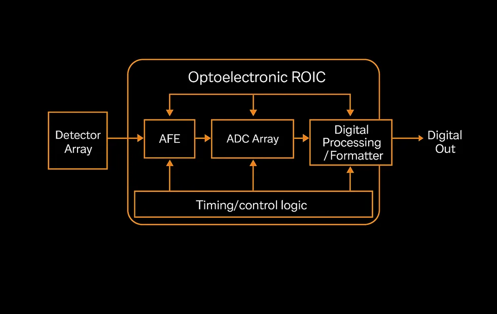
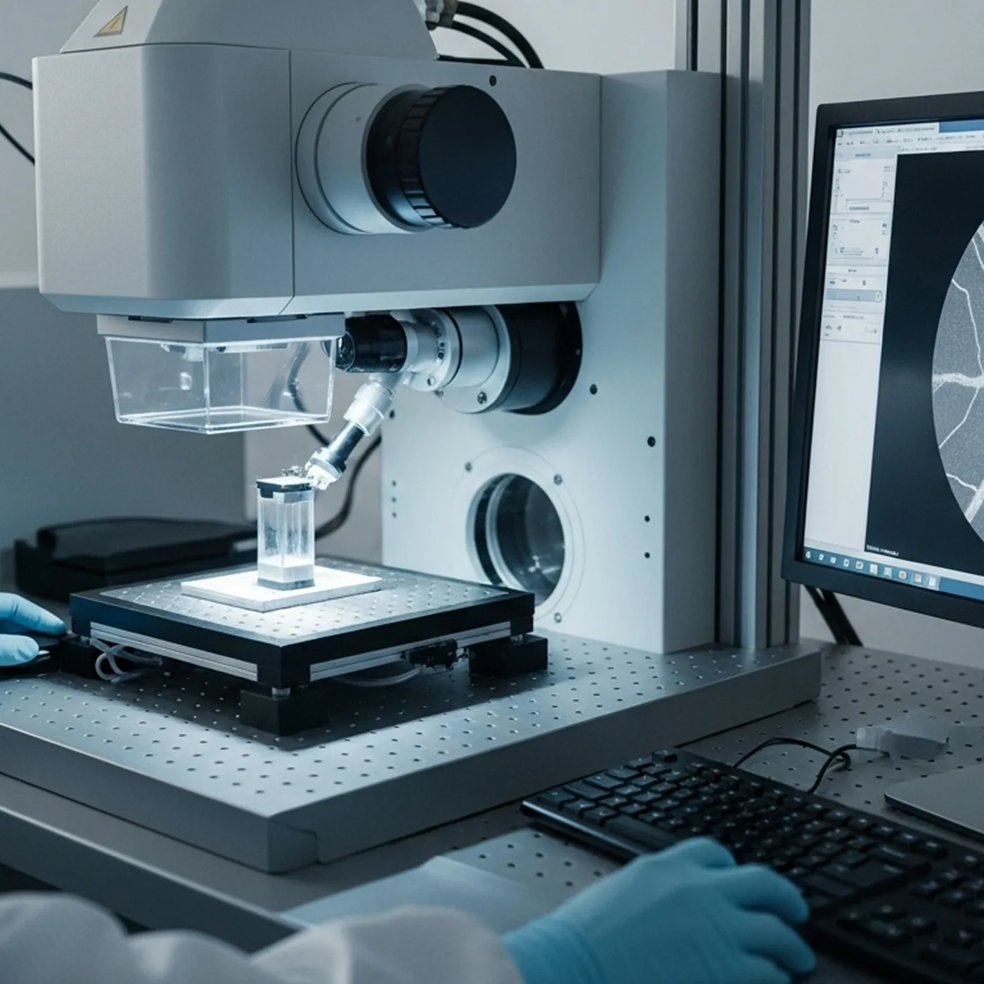
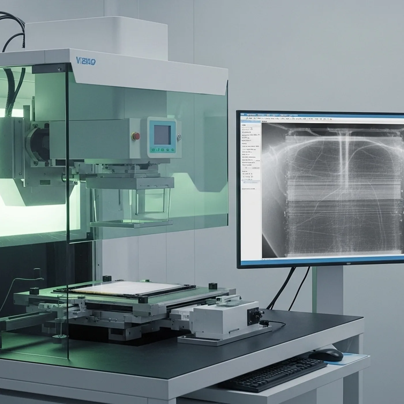
Versatile Pixel Architecture (10–200 μm+)
Configurable pixel pitch for X-ray, thermal, IR (InGaAs/Ge/Si), and low-photon scientific detectors. Customizable full-well, sensitivity, and dynamic range to match detector requirements.
High Dynamic Range & Ultra-Low-Noise AFE
Advanced AFE for extreme illumination differences and weak-signal capture, with ultra-low noise, low-power operation, and temperature-stable performance for industrial, automotive, and scientific environments.
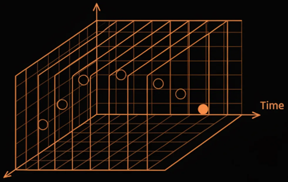
Frame Fidelity + Event-Driven Intelligence
High-quality frame-based readout with integrated event sensing for motion-blur reduction, instant anomaly detection, and low-latency response. Hybrid frame + event architecture enables neuromorphic performance in X-ray and IR systems.
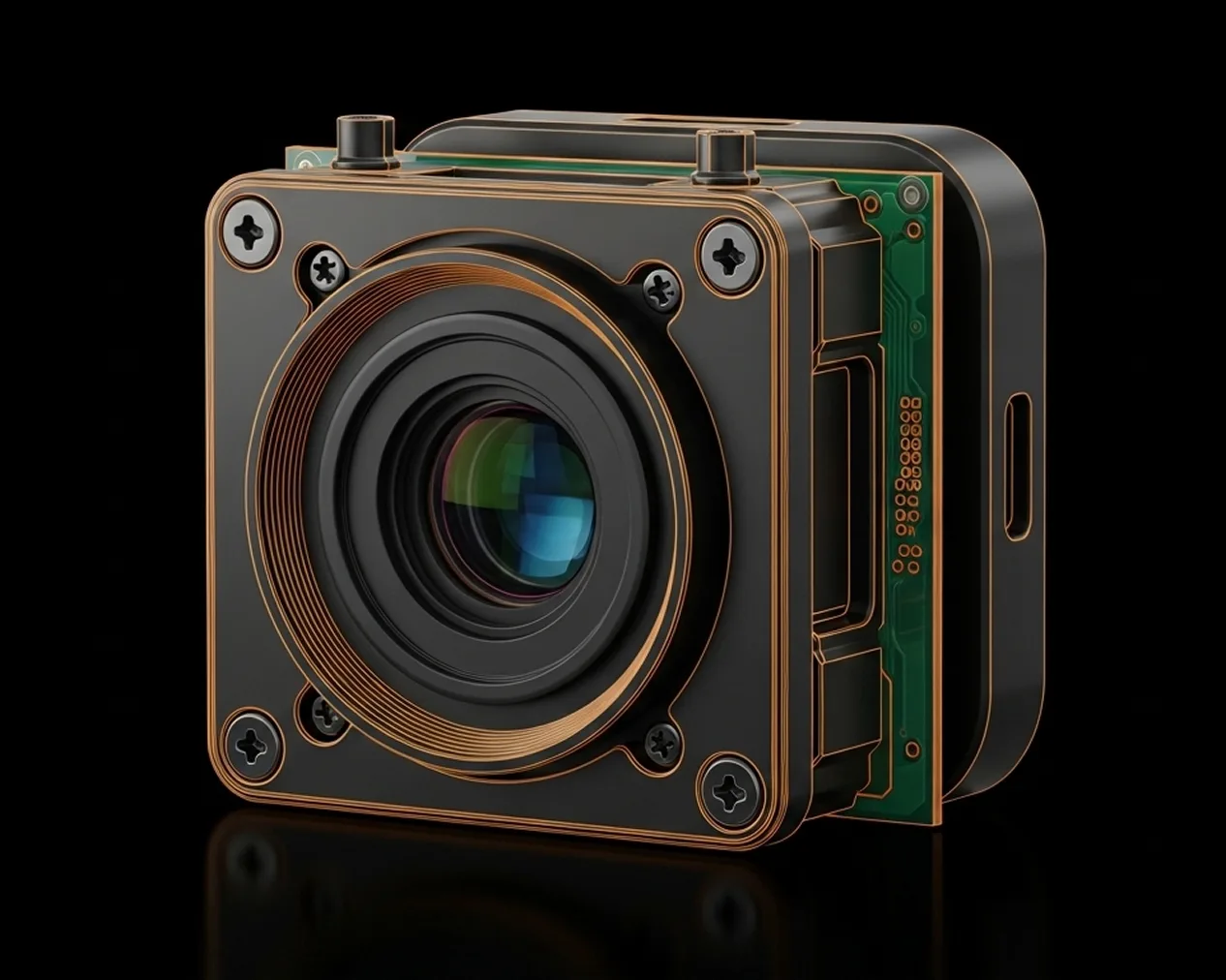
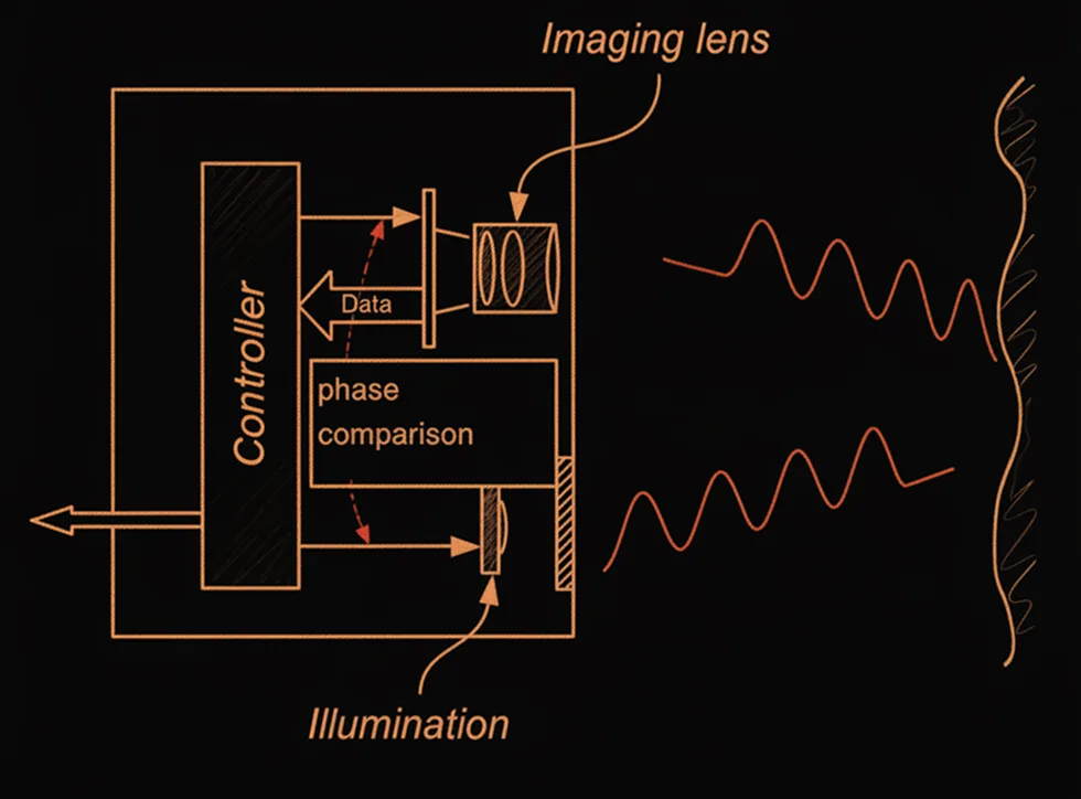
Multi-Mode & Configurable Readout Pipeline
Supports integration, snapshot, rolling, and global modes with configurable gain, timing, and bias. Offers column-parallel or distributed ADC options in stacked or planar processes with custom CFA/micro-optics.
Hybrid ROIC with Integrated EVS
Pixel-level event triggering, regional motion/anomaly flags, and EVS + frame fusion for intelligent perception. Efficient low-data-rate outputs via LVDS / SPI / MIPI.
System Integration & Software Ecosystem
Standard interfaces (MIPI, LVDS, SPI, DVP) with built-in calibration, compensation, and self-test. Includes SDKs for reconstruction, thermal enhancement, motion/anomaly detection, and hybrid event fusion for rapid SoC deployment.
Advantages of ROIC
- Wide dynamic range tailored for extreme contrast imaging (X-ray, IR, photon counting).
- Ultra-low noise enabling detection of weak or low-photon signals.
- Frame + event fusion, delivering neuromorphic responsiveness in traditionally frame-only domains.
- Low power consumption, ideal for portable, battery-powered, and 24/7 monitoring systems.
- Broad detector compatibility, from scintillators to microbolometers to InGaAs arrays.
- Flexible architecture scalable across pixel sizes, ADC types, and wafer processes.
- High integration with mainstream SoCs through standard and custom interfaces.
Applications


- Medical & dental X-ray detectors.
- Security and NDT X-ray inspection systems.
- Infrared thermal cameras for automotive & industrial sensing.
- AIoT thermal monitoring, smart building systems, and predictive analytics.
- Scientific and laboratory detectors requiring precision and low noise.
- Hybrid thermal + event-driven intelligent perception systems.
Cookies
We use cookies to enhance your browsing experience, analyze traffic, and improve our services. You can click “Accept All” to accept all cookies, “Reject All” to reject non-essential ones. For more details, see our Privacy Policy.
Accept All
Reject All